Big Island GPU – A brief architecture overview
Originally published on February 10th 2021
The Tianshu Zhixin was established in Nanjing in 2015 and having R&D centers in Nanjing, Shanghai, Silicon Valley, and Beijing. In 2018 the company officially established a chip development team and began the development of their Big Island architecture, having finally completed its design and entered the manufacturing phase in 2021. Over the years the company has changed its name several times and this has made it very difficult to search for its patents, so the information presented in this article is still preliminary, requiring further research.
Moreover, it was significantly difficult to seek the timeline of events around the company, such as the hiring of several specialists from AMD, Nvidia and Fujitsu, additions that made its design team one of the best and most complete design teams in China. Adding all linguistic difficulties and poor official information it’s no wonder few have taken an in-depth look at the GPU announcement.
A configurable hybrid heterogeneous computing core architecture
The basic concept behind the Big Island architecture is to achieve maximum flexibility and high computational power through the combination of features found between GPUs and TPUs, forming a configurable hybrid heterogeneous computing core architecture for multi-field AI applications.
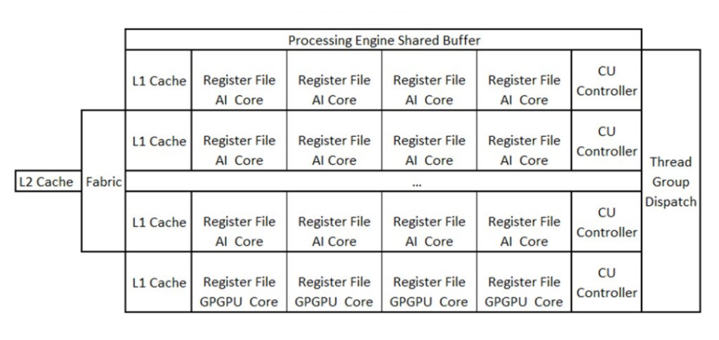
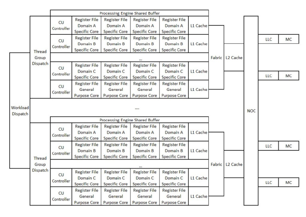
The hybrid processing engine is formed by a thread group scheduling module capable of splitting the workload into several thread groups and sending each thread group to a specific field computing unit of a designated application for execution.
Each domain specific computing units (DSCUs) are optimized for a specific application, as in the example explained in the patent for a core aimed at accelerating AI convolutions. Also, in each processing engine there is a certain amount of cores that are specifically designated for GPGPU, it being provided in the patent that the proportion of the amount of DSCUs and GPGPU cores can be changed according to different market requirements. At this point, the patent does not offer any real tip about the exact amount of possible DSCU and GPGPU cores present in the final product.

The CU controller is used to read shaders and decode instructions, and then send the instructions to specific cores in each domain for execution, and in each domain-specific core there are separate register files, and a set of register files in each domain-specific computing unit and domain-specific cores share the L1 cache.
To share data between DSCUs, buffer store/load instructions are used to send data into or get data from the Processing Engine Shared Buffer (short access latency) or L2 cache (large access latency). The shader has many instruction statements, and different statements are executed in different DSCUs. A special command is used to notify the CU controller to move the thread group to another DSCU. Such an instruction is embedded at the end of each statement to let the CU controller complete the switch.
It is important to note that when reference is made to domain specific computing units, such units are not just limited to AI acceleration. An example of DSCU given in the patent which may be present in the final product is an ASIC core responsible for end-to-end data manipulation, where this specific core is designed for data loading, query, connection, aggregation, and filtering. In this way, it is possible to state the architecture presented by Tianshu Zhixin is an aggregate of accelerators together with a flexible GPGPU platform suitable for multiple AI applications domains where each domain has its own specific core which can solve problems efficiently.
In other words, what is proposed in the Big Island architecture is that in each processing engine different numbers of DSCUs can be configured according to the requirements of different fields, and then the number of processing engines can be expanded to achieve a corresponding performance level for different market fields. In this architecture, it would be possible to focus on the design of new computing units in specific areas for emerging algorithms and add this DSCU to create new products. Under this architecture, using DSCU as a building block can shorten project design time and quickly and efficiently create products required by the market.
It would be very interesting to enter now into a more detailed analysis of the implementation of the fabric that will be used in this architecture – of which the patent is already in my hands. However, given the purpose of this article and the number of patents that still need to be analyzed on this architecture that topic will be detailed in a future article.
A Real Concern
The possibility of losing the huge market share corresponding to the Chinese market coupled with increasingly evident high-tech self-sufficiency that has been emerging in China in multiple fields will be a real cause for concern for all Western tech companies in the coming years.
Big Island is an excellent example of the long-term strategic vision aimed at serving China’s growing AI and Cloud market, with deployment expected very soon. Adding the great versatility and the innumerable possibilities for evolution of the architecture to the in-house Chinese developments of other important elements such as advanced node technology and DRAM fabrication, it is possible to see clearly a not-too-distant future in which Tianshu Zhixin becomes a global name in AI innovation. It will be interesting to follow the evolution path of Big Island and how the incumbent GPU makers will respond.
Some references and reading recommendations
CN110659118A – Configurable hybrid heterogeneous computing core architecture for multi-field chip design – 邵平平 – Tianshu Zhixin – [link] – Chinese only
Iluvatar CoreX press release – Tianshu Zhixin successfully lights up the 7nm process GPGPU cloud training chip with twice the performance of mainstream products in the market – [link] – Chinese only


